Lasers Shaping the Nanoworld
Hybrid, micro-ring resonator devices photo-imprinted on optical fibres (ULF-FORTH, Greece)
Integration and robustness are cornerstone characteristics for the fabrication of photonic devices in both planar and fibre geometries. This presents major challenges to the “Lab-in-a-Fibre” protocol, where multi-functional, miniaturised devices are implemented in microstructured optical fibres [1]. A great functionality optical element is the micro-ring resonator (MRR), while being used in routing and sensing photonic devices, realised in the integrated planar waveguide geometries. There are only a very few examples of MRR devices created on optical fibres, since the fabrication obstacles remain significant. This combina- tion will allow the development of a new kind of photonic device combining the advantages of both the fibre and planar geometries, with connectorisation, miniature size, robustness and integration capabilities.
Researchers at ULF-FORTH have recently demon- strated a new type of miniaturised MRR device, directly imprinted onto micrometric optical fibre tapers (OFTs) [2] using sub-micrometre resolution multi-photon lithography (MPL). Using the three-dimensional character of the MPL [3] enabled the precise imprinting of MRRs with typical diameters of tens of micrometres and sub-micrometre transverse ring dimensions (see figure). These OFT-MRR photonic devices operate in the 1.5μm spectral band, with the OFTs drawn from standard telecom optical fibres, and exhibited light resonance with Q-factors up to ~104 (figure inset). This was achieved by tuning the MRR diameter and its waveguiding characteristics using 3D printing. OFT- MRRs were demonstrated in new ultrasensitive ethanol vapour sensors, readily achieving sensitivities better than 0.5ppm, by exploiting surface physisorption effects.
More complex OFT-MRR configurations include concatenated, scissor-shaped, or cross-coupled resonators, which were investigated for their gas pressure and nano- position-sensing functionalities, based on modal hybridisation effects. Investigation of the opto-mechanical excitation of those MRRs for the colocation of light and acoustic modes has also been carried out. A fundamental objective of the approach is the use of the powerful MPL technique for rapid-yet-precise prototyping of high optical performance OFT-MRRs with good packaging and portability prospects, for translation into field applications. This design and fabrication approach aspires to set a paradigm for photonic components developed as part of Industry 4.0.
Vasileia Melissinaki, Odysseas Tsilipakos, Maria Kafesaki, Maria Farsari, Stavros Pissadakis (ULF-FORTH)
[1] S. Pissadakis, Microelectron. Eng. 217: 111105 (2019)
[2] V. Melissinaki et al., IEEE J. Sel. Top. Quantum Electron. 27: 1-7 (2021)
[3] M. Farsari, B. N. Chichkov, Nature Photonics 3: 450 (2009)
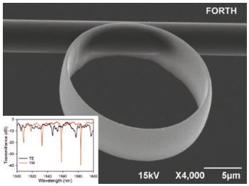
SEM picture of a 20μm diameter MRR imprinted using MPL onto a 2.2μm diameter OFT. Inset: Transmission spectrum of this OFT-MRR for transverse electric (TE) and transverse magnetic (TM)
polarisation states.
Shaken, not stirred: a recipe for spin switching (FELIX, the Netherlands)
For the first time, an international team of scientists has demonstrated magnetisation switching triggered by the vibrations of a crystal lattice. Small perturbations can have a profound effect on macroscopic systems, an unfortunate example being the Broughton and Angers bridge collapses in the mid-1800s caused by the resonant vibrations of soldiers marching in unison. Similarly, in condensed matter systems, small excitations can have large repercussions on both ground and excited states.
Researchers from FELIX Laboratory and the University of Bialystok, in collaboration with scientists from the Institute for Molecules and Materials, Delft University of Technology, and the Max Planck Institute for Solid State Research, have found a way to convincingly demonstrate for the first time a constructive use of these excitations.
The team used short, intense pulses from the FELIX free electron laser to show that “shaking” the atoms in a crystal for a short time can lead to a permanent switching of magnetisation polarity. The FEL is ideally suited to fit the resonance frequencies of the chosen lattice. Following the excitation, nonlinear interactions in the phonon system change the potential landscape of the magnetic system, forcing it to evolve into a peculiar four domain pattern. “It has been discussed for years that such switching in prin- ciple could be possible, but has only now been realised, thanks to the high intensity and narrow bandwidth of the FELIX pulses” explains Andrei Kirilyuk.
Ultrafast modification of the crystal field environment has the potential to become the most universal way to manipulate magnetisation, and it could be a starting point for innovative IT concepts, such as ultrafast optospintronic devices.
Andrei Kirilyuk (FELIX)
A. Stupakiewicz et al., Nature Physics 17: 489 (2021)
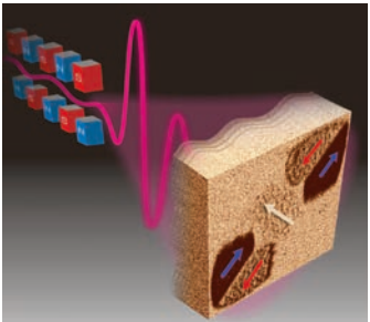
Four-magnetic-domain pattern switched by a FELIX pulse.
Image: A. Stupakiewicz
Lasers for nanolithography (LaserLaB Amsterdam, the Netherlands)
In the past decades, technology has developed to a point where integrated circuits (ICs) – highly sophisticated man- made nanostructures – underpin household devices such as smartphones and drive progress in virtually every form of advanced technology. The semiconductor industry has been continuously innovating their production capabilities at a stunning rate, doubling the transistor density on an IC every two years (Moore’s law). While this is an empirical observation, it is driven by a fascinating array of physics research. Particularly interesting is photolithography, in which light is used to image a mask onto a wafer. The mask contains the structures to be printed, while the wafer contains a photosensitive layer that gets exposed to the light in just the right places. After exposure, the wafer is processed to turn the printed structures into a final device. These steps are repeated many times to produce a modern IC.
To successfully produce nanostructures with such a lithographic process is a daunting task, with a range of op- tical-physics-related challenges. The Advanced Research Centre for Nanolithography (ARCNL) in Amsterdam per- forms fundamental research with an application perspec-tive into lithography. The ARCNL research programmes have close ties to Laserlab-Europe partner LLAMS at the Vrije Universiteit. A large part of the research at ARCNL involves light and lasers. Next-generation lithography machines based on extreme-ultraviolet (EUV) radiation are becoming a reality, employing a laser-produced-plasma (LPP) based source to produce EUV radiation. Such LPPs present a rich research area in which laser science, atomic spectroscopy and plasma physics come together. In addition to the light used for lithography itself, light also plays a crucial role in metrology: to print a nanostructure in exactly the right position with nanometre accuracy involves an array of laser-based measurements, including optical imaging, coherent diffraction, and ultra-broadband scatterometry.
These techniques are fast, non-invasive and can reach sub- nanometre positioning resolution through phase-sensitive detection. Therefore, at ARCNL we have established re- search programmes including digital holographic microscopy, lensless EUV imaging, imaging in scattering media, and attosecond spectroscopy with high-harmonic generation sources.
Stefan Witte and Oscar Versolato (LLAMS/ARCNL)
F. Torretti et al., Nature Communications 11: 2334 (2020)
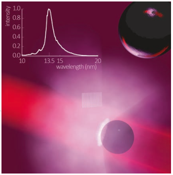
LPP formed by the irradiation of liquid tin microdroplets by high-energy ns laser pulses.
The hot, dense plasma generates extreme ultraviolet light near 13.5 nm, relevant for state-of-the-
art nanolithography.
Image: Tremani/ARCNL, from Nature Communications 11: 2334 (2020)
Using femtosecond laser pulses to modify bimetallic nanoparticles (CLUR, Spain)
Nanoscience and nano- technology, in particular, the strong interaction of conduction band electrons of noble metal nanoparticles (NPs) with electromagnetic radiation, have great interest for catalytic, plasmonic and magnetic applications. This interaction gives rise to localised surface plasmon resonances (LSPRs), producing novel optical, electrical and magnetic properties. Silver has a higher plasmonic activity than gold, but its chemical instability is an important drawback. One promising strategy to overcome this is using Au-Ag alloys [1], but their controlled formation is not a trivial task.
Scientists at the Center for Ultrafast Lasers (CLUR) have used a novel approach, based on the fabrication of Au@Ag core-shell structures via wet chemistry and their irradiation with 800 nm fs pulses to induce melting and alloying [2] (Figure A). The energy transferred to the nanostructure by the laser pulses thermally activates the Au and Ag atoms, which enhances diffusion and causes mixing and alloy formation. Both the deposited energy and the heat dissipation rate play an important role in the shape and distribution of the metals in the final alloyed nanostructure [2]. Hence, Au@Ag nanorods can be reshaped to produce diverse novel nanostructures just by controlling the pulse fluence and the surfactant concentration. At low fluences, the core-shell structure is maintained, and only slight re- shaping is observed, mostly at the tips (Figure B). Increasing the fluence to 6.4 J/m2 formed rice-like NPs, as well as other structures (Figure C). Partial alloying was confirmed by HAADF-STEM tomography and EDX tomography. This effect was more evident at 33.28 J/m2 (Figure D), and at 92 J/m2 (Figure E) we obtained completely alloyed NPs. This technique enables the partial or complete alloying of Au@ Ag nanoparticles in a simple and reproducible manner, with potential applications in other heterostructures. The main requirements are the ability of such nanoparticles to absorb laser light (either via excitation of LSPRs or inter- band transitions), and the availability of fs-laser pulses with the desired wavelength and fluence. This methodology is expected to provide novel routes for synthesising colloidal bimetallic alloy nanoparticles with precise control over their size and composition.
Luis Bañares (CLUR), Andrés Guerrero-Martínez (Universidad Complutense de Madrid) and Ovidio Peña-Rodríguez (IFN, Universidad Politécnica de Madrid)
[1] G. González‐Rubio et al., Adv. Opt. Mater. 9: 2002134 (2021)
[2] G. González-Rubio et al., Science 358: 640-644 (2017)
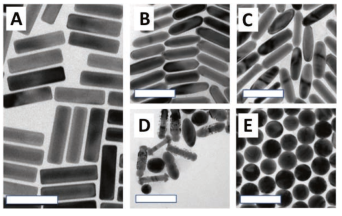
TEM micrographs before (A) and after irradiation with fluences of (B) 3.2 J/m2, (C) 6.4 J/m2, (D) 33.28 J/m2 and (E) 92 J/m2. Scale bars: 100 nm.
Image: CLUR
Laser crystallisation of titanium dioxide nanotubular layers for photo- voltaic applications (HiLASE Centre, Czech Republic)
With the increasing world population, biocompatible and green-chemistry-based sustainable energy sources, air purification and waste-water treatment plants are increasingly important. Photocatalysts, particularly TiO2, are of interest, for example in dye-sensitised solar cells or air and water purification. Most of these applications involve nm- scale TiO2 structures. Anodic TiO2 nanotube (TNT) layers are very promising, comprising several-μm arrays of nanotubes with a diameter of 90-100 nm.
Highly-ordered anodic TNT layers can be grown in fluoride-ion-containing electrolytes. However, the as-formed TNT layers are amorphous. For photocatalytic applications, the crystalline structure is a crucial parameter, with anatase being the typical preference. This is usually produced via thermal annealing, which is both time- and energy-con- suming. Laser annealing is relatively quick and can offer localised annealing of TNT layers, but the resulting layers are usually molten on top.
The HiLASE Centre, in collaboration with the Centre of Materials and Nanotechnologies (University of Pardubice, Czech Republic) have achieved laser crystallisation of an- odic amorphous TNT layers into the anatase phase [1]. The process takes around 14 minutes and the resulting anatase TNT layers do not show any signs of deformation or melting.
This was achieved with the combination of high energy per pulse, ultrashort pulse duration (~2 ps), and high repetition rate available on HiLASE Perla-C. The crystals formed via explosive solid-phase crystallisation, which is ignited by the laser-induced stress wave formed in the light absorption zone on the top of the TNT array, and which propagates one-dimensionally along the nanotubes. Careful analysis of the absorbed energy, initial temperature rise, and stress amplitude supports this crystallisation process.
The laser-annealed TNT layers were found to have a lower overpotential for hydrogen evolution (important for hydrogen-based electrochemistry) than oven-annealed TNT. XPS spectra similarly show a better surface stoichiometry. Photo-electrochemical measurements reveal that the laser annealed TNT layers contain more defects than the oven annealed TNT layers, resulting in lower photocurrent densities, a lower flatband potential and higher donor concentration.
The new process is fast and clean, avoiding oxidation of the underlying titanium substrate and allowing patterned crystallisation in localised areas. The new under- standing of the high-power-laser crystallisation process opens methods for non-destructive laser annealing of other amorphous semiconductor structures.
Inam Mirza, Nadezhda M. Bulgakova and Tomáš Mocek (HiLASE Centre)
[1] H. Sopha et al., RSC Adv. 10: 22137-22145 (2020)
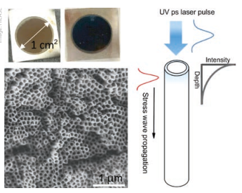
Left: Initial and laser-annealed TNT sample (1 cm2) and its magnified view, demonstrating the absence of any signs of melting or deformation. Right: a schematic of the laser-induced solid phase crystallisation.
Image: HiLASE
Nanostructured materials to improve the efficiency of laser-driven ion sources (LLC, Sweden)
Achieving a tunable, reliable source of ion beams would facilitate scientific, technological and possibly medical break- throughs. For the past two decades, a particularly active research field has been the theoretical understanding and experimental control of ion beams produced by focusing an intense, ultrashort laser pulse onto thin solid targets.
A major challenge is to increase the conversion efficiency from laser energy to ions. For this, a well-established strategy consists of adding nanostructures to the surface of the irradiated target, typically a few-µm-thick metallic foil. Different shapes, sizes and arrangements of the na- nostructures can favour the acceleration processes and in turn produce ion beams with higher energies when compared with simple flat foils.
In this context, recent studies of proton acceleration from nanostructured targets (see figure) have been performed at the Lund Laser Centre (LLC) in collaboration with researchers from Institut de la Recherche Scientifique INRS-EMT of Varennes (Canada) [1] and the University of Gothenburg (Sweden) [2]. Targets consisted of thin foils with the surface either covered with a forest of nanowires or perforated with nm-scale holes. Together with numerical simulations, the experimental results allowed exploration of the role of different geometrical parameters, validation of the efficiency of the structures, testing of manufacturing inaccuracies, and better understanding of the conditions of laser-plasma formation that affect the final energy of the proton beam.
Besides target design, fabrication and metrology are crucial for achieving reproducible ion beams. At the laser intensities required for plasma acceleration (>1018 W/cm2), targets are ablated and must be renewed after each shot, and their availability becomes even more relevant for the development of laser-driven sources with a high repetition rate (1-10 Hz). This clearly adds a challenge to the many different fabrication techniques (coating, lithographic, mechanical, chemical), which must deliver large quantities of targets with consistent structures. Realistically, there will be a trade-off between ion acceleration efficiency and cost-effectiveness.
For these reasons, ion acceleration from nanostructured targets joins expertise from the domains of laser-plasma interaction, photonics, materials science and nano-engineering. Innovative designs and high reliability remain key for pushing forward the understanding and optimisation of laser-driven ion sources.
Giada Cantono (LLC)
[1] S. Vallières et al., Sci. Rep. 11: 2226 (2021)
[2] G. Cantono et al., Sci. Rep. 11: 5006 (2021)
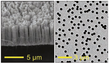
Nanostructured targets used at LLC to accelerate proton beams.(Left) Cu nanowires grown by electrochemical deposition on 300 nm-thick Au substrates. (Right) 200 nm-diameter nano-holes in 100 nm-thick Au foil, realised with hole-mask colloidallithography.
Partially modified from [1] under CC BY 4.0.
Ultrafast skyrmion reshuffling (MBI, Germany)
Smaller, faster, more energy-efficient: future requirements for computing and data storage are hard to fulfil and alternative concepts are always being explored. Particle-like magnetisation patches that form very small swirls in an otherwise uniformly magnetised material, called skyrmions, show great potential for novel memory and logic devices. Skyrmions are stable at room temperature, with diameters down to the 10-nm range. To be considered for practical application, however, fast and energy-efficient control of these nanometre-sized skyrmions is required.
A team from the Max Born Institute, Helmholtz-Zentrum Berlin, Massachusetts Institute of Technology and others have investigated in detail how laser-based “skyr-mion writing” can be controlled for use in devices. Sub-ps laser pulses, applied in the presence of an external magnetic field, can be used to write and erase them. This provides a faster and potentially more energy-efficient route than previous electrical methods. To image the skyrmions, holography-based x-ray microscopy was used, which can visualise the tiny magnetisation swirls.
There is a material-dependent window of laser intensities which permits the creation of a new skyrmion pattern which is completely independent of the previous magnetic state. Remarkably, the number of skyrmions created within the laser spot is not influenced by the laser intensity but by the external magnetic field, which can be precisely controlled. The strength of the external field therefore provides a “tuning knob” for the number of skyrmions created and even allows for annihilation of skyrmions [1]. The controlled creation or annihilation of single skyrmions within the laser spot was also demonstrated, representing the writing of a single bit.
The creation of a tunable skyrmion spot, independent of the prior magnetic state, is of interest for potential future devices since it could be used as a “skyrmion reshuffler” for stochastic computing. Stochastic computing represents numbers by strings of random bits with a given length, and with the probability of encountering “1” encoding the number value. Computations can then be carried out via logic operations between the individual bits within a string. However, completely randomised bit strings are needed in order to obtain correct results. The skyrmion reshuffling in this project was on the picosecond timescale, which is compatible with state-of-the-art computer clock speeds and is much faster than in previous efforts based on thermal diffusion (operating on the second-timescale).
Bastian Pfau and Rebecca Davenport (MBI)
[1] K. Gerlinger et al., Appl. Phys. Lett. 118: 192403 (2021)
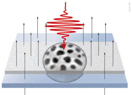
A single laser pulse of appropriate intensity can create random skyrmion patterns, with density
defined by an external magnetic field (arrows). This can be used as an ultrafast “skyrmion reshuf-
fler” for stochastic computing. The dashed circle marks the field of view of the x-ray holography
microscope used to see the magnetic skyrmions (appearing as black dots), 1 µm in diameter.
Image: MBI
Microtargetry for the Nanoworld (CLF, United Kingdom)
The Central Laser Facility at the STFC Rutherford Appleton Laboratory has been supported by a Target Fabrication Group since its beginnings over 40 years ago. The targets that are supplied allow the exploitation of the facilities’ high-power lasers to study fundamental physics such as shock propagation, particle acceleration and x- ray generation. Over the last decade this targetry has become more complex, with tolerances and specifications now regularly required at the nm level.
The dedicated team of scientists and engineers in the Target Fabrication Group are bringing capabilities on-line to meet these challenges and have recently invested in single point diamond turning (SPDT), advanced deep reactive ion etching for processing silicon wafers (DRIE), nanowire growth for increased laser absorption onto targets, and a suite of precision laser micromachining systems that are operated by its spinout company Scitech Precision Limited.
Targets that can be fabricated using these advanced capabilities include sine-wave ‘rippled’ structures for the investigation of Rayleigh–Taylor instabilities. The features have periods of a few tens of micrometres and amplitudes of approximately 5 micrometres with Figure 1 showing a complex dual mode structure. The structures are often part of a more complex assembly with the target in Figure 1 showing a tube containing microstructured plastic foam through which material from the ripple target propagates. In addition to targets, complex structures such as fine meshes in hard-to-machine materials can be laser mi- cromachined. The example in Figure 2 shows a niobium mesh supporting a thin-film filter for space applications. It was machined from a 50 micrometre foil with arm thicknesses as thin as 40 micrometres.
Targetry will be the limiting factor in fully exploiting the latest developments in laser technology, so the move to higher volume production is the challenge for the next decade.
Christopher Spindloe (CLF)
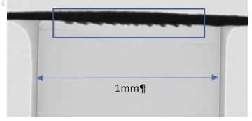
Figure 1: Structured foil as part of a complex RT target. The dual-mode structure can be seen on the rippled foil. The tube diameter is 1mm and the ripple target is highlighted.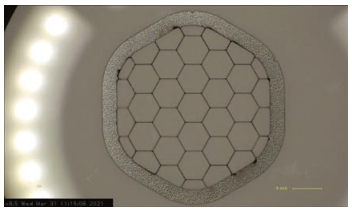
Figure 2: A niobium mesh micromachined using a 1033nm fs laser to provide a support for a thin film filter.
Images: CLF
Femtosecond laser pulses modify the properties of 2D materials (Laserlab- NSC, Finland)
It is expected that 2D materials will become commonplace in electronic devices over the coming decade. One of the central obstacles to this development is modifying the properties of 2D materials to improve their performance.
Researchers at Laserlab-NSC have shown that photons can be used to modify the electronic, optical, chemical, and mechanical properties of 2D materials. The key to successful laser-induced material modification is the combination of femtosecond pulses and fluences just below the ablation threshold. Two distinct processes were obtained using direct laser writing with femtosecond laser pulses.
Irradiation of graphene under inert atmosphere forms localised defects, inducing strain and causing the graphene to bulge out of plane. This effect can be used to write 3D structures with sub-diffraction-limited features on graphene/SiO2/Si [1] and other 2D materials, such as MoS2 [2]. Higher doses lead to line defect formation and activation of luminescence via the formation of small graphene “islands”, mimicking carbon nanodot material [3]. The rippling phenomenon induced on suspended graphene increased its stiffness by several orders of magnitude [4].
When specimens are irradiated under ambient atmosphere, the oxygen-containing groups are incorporated into the graphene lattice. This process enables the laser writing of oxidised areas on graphene. The oxidation opens a band gap, which is beneficial for electronic circuit fabrication. Additionally, the oxidised areas can be used for selective adsorption of molecules, as was demonstrated for protein immobilisation [5].
These methods provide a great toolbox for the optical writing of electronic circuits and device fabrication. Furthermore, the possibility to combine them with area- selective chemical functionalisation of 2D materials is promising for the development of biosensors and other devices.
Mika Pettersson and Kamila Mentel (Laserlab-NSC)
[1] K. K. Mentel et al., Nanoscale Adv. 3: 1431 (2021)
[2] M. T. Turunen et al., Adv. Mater. Inter. 8: 2002119 (2021)
[3] V.-M. Hiltunen et al., J. Phys. Chem. C 124: 8371 (2020)
[4] V.-M. Hiltunen et al., NPJ 2D Mater. Appl. 5: 49 (2021)
[5] E. D. Sitsanidis et al., Nanoscale Adv. 3: 2065 (2021)
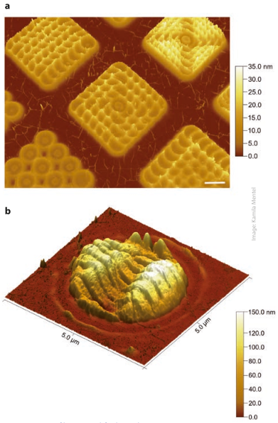
AFM images of laser-modified graphene. (a) 3D patterns prepared on monolayer graphene on Si/SiO2 substrate. Scale bar 1 µm. (b) Laser-induced ripples on suspended monolayer graphene. The sample was fabricated by etching a round hole on a SiN membrane and transferring graphene onto it.
Image: Kamila Ment
Laser nano-printing of 3D crystalline structures (VULRC, Lithuania)
A novel route for laser nano-printing of 3D crystalline structures has been developed, employing ultrafast laser lithography – used as additive manufacturing tool for producing true 3D nanostructures – and combined with high temperature thermal post-treatment, converting the printed material into a fully inorganic substance.
This interdisciplinary experimental work was performed by a group of applied chemists and laser physicists at Vilnius University. They revealed the potential of tuning the sintered ceramic structure into distinct crystalline phases, including cristobalite, SiO2, ZrSiO4, m-ZrO2, and t-ZrO2.
In the systematic study, the starting model material was SZ2080™, and its derivatives containing variable fractions of Si and Zr were used to tune the resulting phases of the crystalline nanostructures. The laser fabricated and calcinated structures experienced downscaling in dimension towards 40-90% of their initial volume, yet perfectly preserving the designed 3D architectures, including porosity. The sintering process ensured complete removal of organic substances and re-arrangement of the material into glassy or crystalline ceramic matter. With more zirconium, the inorganic material is achieved at a lower temperature. The strong adhesion to the quartz or corundum substrates and high robustness in both high and cryogenic temperatures was validated by flushing the 3D nanostructures directly with liquid nitrogen down to -196°C for 10 min and letting it evaporate freely. No de- tachment, delamination, or fracture of the structures was observed. The process and outcome are summarised in the figure.
This approach achieved sub-60 nm individual 3D features without any beam shaping or complex exposure techniques, thus makes it reproducible with other laser direct writing setups. The principle is also compatible with commercially available platforms (including Nanoscribe, MultiPhoton Optics, Femtika, Workshop of Photonics, Up- Nano, MicroLight).
The validation of the combined laser manufacturing and thermal-treatment technique upgrades the widespread laser multi-photon lithography process to create a powerful tool enabling additive manufacturing of crystalline ceramics at unprecedented precision and three- dimensional flexibility. This breakthrough is a milestone significantly contributing towards advancing the field of future opto-electronics.
Darius Gailevičius and Mangirdas Malinauskas (VULRC)
[1] G. Merkininkaitė et al., Opto-Electron. Adv. 5: 210077 (2022)
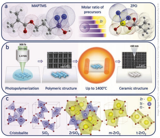
A graphical summary showing: (a) raw organic and inorganic precursors and their molar ratios in synthesis (b) laser photopolymerisation and high-temperature calcination technology (c) resulting crystalline phase nano-lattices after calcination. These can all be observed and tuned depending on the treatment temperature and initial hybrid material compositions.
Image: Figure from [1], used under Creative Commons license CC-BY 4.0

