Lasers Exploring the Nanoworld
Ultrafast transient holographic microscopy (POLIMI, Italy and ICFO, Spain)
Observing ultrafast light-matter interactions at the nanoscale is of great interest for tracking energy flow in semiconductors or for the study of dynamics in single nanoparticles or even single molecules. This is technically challenging, and most approaches so far have relied on single-point detection, employing raster scanning of a tightly focused beam on the sample to achieve large observation areas. Researchers at ICFO and POLIMI have recently combined ultrashort pulses with off-axis holography to develop a new transient scattering technique that can measure the ultrafast response of hundreds of nano-objects within a wide volume-of-view of around 100×100×100 μm 3 [1].
The reported approach relies on a dark-field scattering microscope illuminated by 100-fs pulses. While such a microscope can produce wide-field scattering images of the sample in steady state, turning it into a transient mi- croscope usually runs into the problem that cameras have slow frame rates, limiting the ability to modulate a pump beam at high frequencies to achieve sensitive detection. This issue was solved by introducing two off-axis reference beams generated using a 2D grating that interfere with the image at the camera. A 2D Fourier transform of the result- ing image pattern neatly separates the interference of the sample image with either reference beam in k-space. By modulating the references synchronously with the pump beam, researchers were able to ensure that one reference interferes with the sample image corresponding to pump- on only, while the other with the pump-off only, effectively decoupling the pump modulation frequency from the camera acquisition speed and implementing a wide-field digital lock-in. Therefore, each acquired hologram contains both pump-on and pump-off images, which can be isolated in k-space, Fourier transformed back into real space, and subtracted to obtain the transient response at each pixel of the original image.
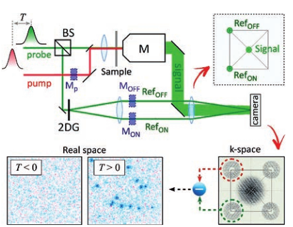
Upper panel: schematic of the multiplexed holographic microscope. BS: beam splitter, M: micro-
scope objective, 2DG: 2D phase grating. Modulators on Ref ON (M ON ) and Ref OFF (M OFF ), respectively
synchronous and asynchronous with the modulated pump beam (Mp), enable recording the
pumped and unpumped images, which are separated by k-space filtering. The data show a
proof-of-concept wide-field ultrafast transient scattering experiment on a distribution of
100-nm gold nanoparticles.
This concept was demonstrated by acquiring tran- sient scattering signals from dozens of gold nanoparticles scattered on a glass surface in a single measurement and highlighting differences in their ultrafast dynamics due to the particle shape or environment. Furthermore, the holographic setup yields both the amplitude and the phase of the signal, allowing the use of digital holography techniques to propagate out-of-focus signals into focus by a simple data processing step. This was demonstrated by acquiring data with the sample deliberately out of focus. Researchers were nonetheless able to propagate both the steady state and transient scattering signals into focus, demonstrating the unique 3D capabilities of this approach. It is hoped that this technique can be a single-shot alternative to current photothermal imaging methods.
Sandro De Silvestri, Giulio Cerullo, Franco Camargo (POLIMI)
[1] M. Liebel et al., Nano Lett. 21: 1666-1671, 2021
Ultrafast nanoscale electron transport in solids (LACUS, Switzerland)
When optoelectronic materials with a high absorption coefficient absorb light, strong spatial charge density gradients develop on a nanometer scale at the surface. Consequently, charge carrier transport and recombination processes set in on a femtosecond (fs) timescale to restore equilibrium. Understanding the microscopic details of carrier evolution is a fundamental prerequisite for developing efficient nano-photonic devices. Some applications, such as solar concentrators, light-emitting diodes and lasers, routinely operate under an extremely high charge carrier density. In this regime, complex many-body phenomena start to play an important role in defining the material’s photophysics, making both the theoretical and technical investigation of their properties difficult. An additional complexity of this ultrafast nanoscale transport stems from its intermediate character between the diffusive and ballistic regimes.
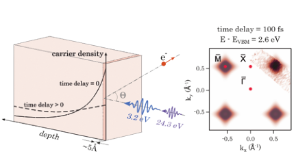
Experimental scheme (left) shows how surface sensitivity of extreme ultraviolet probe pulses
allows to study nanoscale charge transport of a solid (here CsPbBr3) with spatial, momentum,
energy and temporal resolution (right).
While lateral transport characterisation has seen sub- stantial advances owing to recent developments in imag- ing and non-linear optics, the surface-to-bulk transport has not been studied to a comparable degree. In the new study carried out at LACUS, time- and angle-resolved photoelectron spectroscopy (TR-ARPES) with extreme ultraviolet (EUV, 15–50 eV) probe and ultraviolet (3.2 eV) pump pulses was applied on single crystals of the CsPbBr 3 perovskite. The experiment is schematised in the figure. By exploiting the exceptional surface sensitivity of photo- electrons emitted by EUV photons, obtained at the Harmonium light source, the surface electronic population was followed in reciprocal space, providing a sub-nano- metric picture of the light-induced dynamics with fs temporal resolution.
The experimental findings, supported by theoretical modelling of nanoscale carrier diffusion and recombination under strong optical excitation, reveal the super-diffusivity of charge carriers, explainable by the high band velocities of hot carriers within a quasi-ballistic transport regime. The transport was found to asymptotically approach a conventional diffusive regime at the highest car- rier densities even at sub-ps timescales, due to an onset of strong electron-hole scattering, limiting the carrier mean free path. The results showcase the capability of EUV-based TR-ARPES to study ultrafast nanoscale transport with momentum selectivity in crystalline solids.
Majed Chergui (LACUS)
Exploring the stiffness of nano-objects (ICFO, Spain)
The vibrations of the atoms within a solid material are determined by their temperature. When the temperature is higher, the intensity or amplitude of the vibrations is larger. These vibrations directly affect the stiffness of the solid material. Even though scientists are aware of the fact that there is a temperature-dependent change of the elasticity in a single nanoscale system, so far, it still had not been experimentally detected.
In a study published recently in Physical Review Letters, ICFO researchers, in collaboration with the Instituto de Nanociencia y Materiales de Aragón (INMA) of the University of Zaragoza, ICMM-CSIC, Polytechnic University of Marche, TU Delft, and the University of Nottingham, have reported on a new approach to measure the small change in the elasticity of a nanotube when changing its temperature.
In their experiment, the team built a 1-10 micrometre long carbon nanotube, called a cantilever, where one of its ends was attached, fixed to a silicon chip, and the other end was free to bounce around in the air. Next, on the free end of the nanotube, the scientists deposited a tiny amount of platinum to form a particle. Then they placed the entire system within a chamber at room temperature, and while lowering the temperature slowly down to a few degrees Kelvin, they illuminated the nanotube with a He-Ne laser and observed how the system vibrated. They found and measured the vibration mode with lowest frequency, knowing that its motion amplitude was the largest. They observed how the resonance frequency changed to measure the stiffness of the nanotube, which is quantified by the so-called Young’s modulus.
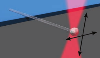
(c) ICFO Schematic illustration of the mechanical resonator with the
platinum particle at the end of the cantilever.
Now, the energy dissipation of resonators is described by the thermal bath, or thermal reservoir, which describes how the resonator is coupled to the outside world. So far, it had been very difficult to identify the microscopic nature of the thermal bath, but in this study, the team was able to show that the thermal reservoir is composed of phonons by a sizeable amount. While lowering the temperature, they saw that the stiffness of the nanotube was dependent on these phonons, that is, the collective excitation in a periodic, elastic arrangement of atoms within the solid. These measurements enable a better comprehension of the physics of mechanical resonators and pave the way to optimising them to reach unprecedented levels of sens- ing precision.
Adrian Bachtold (ICFO)
S. Tepsic et al., Phys. Rev. Lett. 126: 175502, 2021
Polarisation-resolved second harmonic generation imaging microscopy of 2D materials (FORTH, Greece)
The emerging family of graphene and related two-dimensional (2D) materials has provided researchers with fertile ground for exploring fundamental physical phenomena and developing innovative technological solutions. 2D transition metal dichalcogenides (TMDs) MX2 (M: Mo or W, and X: S, Se, or Te) are direct-bandgap semiconductors (structurally similar to graphene), that show electronic and optoelectronic properties, along with desirable mechanical strength and flexibility, offering great promise for use in future electronic devices.
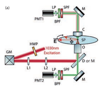
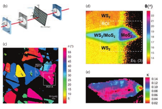
Figure (a) Experimental setup for P-SHG raster-scanning imaging microscopy. (b) Coordinate
system for the theoretical model describing the P-SHG signals from 2D TMDs. (c) P-SHG imaging
of crystal imperfections. (d) Real-time imaging of twist-angle. (e) P-SHG imaging of VPI.
Lately, nonlinear optical measurements, particularly second harmonic generation (SHG) used in conjunction with laser raster-scanning microscopy, have created new opportunities for improving the image resolution of 2D crystals [1, 2] (Figure a). In particular, the SHG signal depends on the elements of the second-order susceptibility tensor χ (2) , which are non-vanishing only for non-centrosymmetric media such as the atomically thin TMDs. At the same time, the polarisation of the SHG field depends crucially on the 2D crystal symmetry and orientation (Figure b).
Based on such SHG signal dependencies, the crystal quality of TMDs can be evaluated using polarisation-re- solved SHG (P-SHG) imaging, with resolution which is lim- ited only by the optical limit of diffraction [1, 2] (Figure c). Moreover, atomically thin TMDs can be assembled in vertical stacks held together by van der Waals forces, enabling interlayer coupling between the layers. This creates new physical properties that depend on the relative orientation (twist angle) between the TMD monolayers. P-SHG imaging microscopy provides accurate and real- time measurement of the twist angle, which is of utmost importance for characterising a 2D TMD heterostructure [3] (Figure d).
Further, degenerate minima in momentum space valleys in 2D materials provide an additional degree of freedom that can be used for information transport and storage. When these atomically thin crystals interact with intense laser light, the SHG field shows special characteris- tics that reflect not only the broken inversion symmetry in real space, but also the valley anisotropy in reciprocal space. This anisotropy is present whenever there exists a population imbalance between the two valleys (VPI). SHG intensity is dependent on the excitation field polarisation. The variation of this dependence with temperature, as revealed by P-SHG imaging, is a unique fingerprint of VPI [4] (Figure e).
Optical P-SHG imaging is envisaged as a powerful tool for the characterisation of 2D TMD heterostructures, and for the engineering of their physical properties for emerg- ing applications.
Sotirios Psilodimitrakopoulos and Emmanuel Stratakis (FORTH)
[1] S. Psilodimitrakopoulos et al., Light Sci. Appl. 7: 18005, 2018
[2] G. M. Maragkakis et al., Opto-Electron. Adv. 2: 190026, 2019
[3] S. Psilodimitrakopoulos et al., 2D Materials 8: 015015, 2021
[4] L. Mouchliadis et al., npj 2D Mater. Appl. 5: 6, 2021
Femtosecond magnetisation dynamics for faster magnetic storage (LOA, France)
Our society’s ever-growing need for computing power requires the regular development of new electronic devices. In the domain of magnetic recording, this translates into faster systems with higher capacities. To go beyond the present state of the art, a deep understanding of femto-second magnetisation dynamics at the nanometre length scale is necessary.
The Sources for Interaction, Imaging & Medical applica- tion group (SIIM) is studying femtosecond magnetisation dynamics in rare earth transition metal alloys, which are promising materials for faster magnetic recording devices [1]. In these materials, the magnetisation dynamic of each component needs to be followed independently. Here, a Co 88 Tb 12 alloy was observed, which exhibits nanoscale magnetic domains. Such a magnetic structure acts as a diffraction grating for the wavelengths corresponding to the absorption bands of Co and Tb. Using the high harmonic source of the Laboratoire d’Optique Appliquée (LOA), femtosecond pulses can be generated spanning the photon energy range of 40 to 70 eV, covering the M2,3 band of Co (around 60 eV) and the O1 band of Tb (around 45 eV). This leads to the appearance of two different scattering spots on a CCD camera set a few centimetres downstream of the sample (see figure, left).
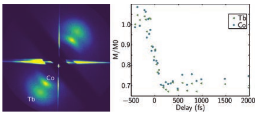
Magnetic scattering pattern of a CoTb alloy film obtained at photon energies between 40 and 70 eV with the high harmonic
source at LOA, showing 2 peaks corresponding to the Co M2,3 bands and Tb O1 band. Following the intensity of these two
edges allow us to follow the magnetisation dynamics of Tb and Co independently on the femtosecond time scale.
LOA researchers have recently studied similar samples at the Free Electron Laser FERMI (Trieste, Italy) and were able to follow for the first time the ultrafast dynamics of the magnetic anisotropy in these alloys, a key parameter that must be precisely controlled for the realisation of magnetic recording devices [2]. Comparing to this study, the work at LOA allows to simultaneously look at the photons in resonance with the Co and Tb bands thanks to the large bandwidth of the high harmonic source. In this particular case, very similar magnetisation dynamics for Co and Tb are observed, contrary to the previous investigations (see figure, right). This on-going work will allow to fine-tune the composition of the alloy and optimise its properties for particular applications.
Boris Vodungbo (Laboratoire de Chimie Physique-Matière et Rayonnement) and Guillaume Lambert (LOA)
[1] C. D. Stanciu et al., Phys. Rev. Lett. 99: 047601, 2007
[2] M. Hennes, Phys. Rev. B 102: 174437, 2020
Transient X-ray grating spectroscopy for nanoscale measurements (LACUS, Switzerland, LENS and FERMI, Italy)
Measuring a variety of transport phenomena at the na- noscale is becoming vital with the miniaturisation of devices. Yet it remains elusive due to the lack of methods which are precise at such length scales. Transient grating (TG) spectroscopy is the traditional tool for measuring transport phenomena. It uses two laser pulses to activate a medium by creating an interference pattern, or grating, from stripes of excitations that can be thermal, electronic, magnetic or even structural. The modulation depth of the grating can be measured by using it to diffract a third, time-delayed probe beam, which monitors the grating evolution as it fades away due as the initial excitation propagates through the material. The grating spacing is determined by the wavelength of the laser pulses used to create it and is on the order of hundreds of nanometres to microns in the visible-ultraviolet range.
Transport properties at the nanoscale are expected to greatly differ from those at the meso- and larger scales. In particular, a change of regime from ballistic to diffusive is known to occur, yet it has not yet been unambiguously observed. Harnessing such nanoscale transport phenomena calls for the use of short-wavelength radiation and, in par- ticular, X-rays. However, crossing two X-ray beams in order to generate a grating with nanometre step sizes is a challenge. In an international collaborative effort led by the Paul-Scherrer-Institut (PSI), Switzerland, and involving several Laserlab-Europe partners (LACUS, LENS and FERMI), the Talbot effect (see figure) was exploited to create such gratings using beams of 0.17 nm wavelength at the Swiss Free-Electron Laser (SwissFEL, PSI). The evolution of the generated grating was probed by a time-delayed 400 nm probe pulse. The results, revealing the optical and acoustic response in the form of coherent phonon oscillations over hundreds of femtoseconds to tens of picoseconds (Figure inset), appeared in Nature Photonics. This first demonstration of hard X-ray transient grating spectroscopy opens the way to novel and exciting developments in the study of na- noscale transport phenomena. The next step will be to replace the 400 nm probe pulse by a hard X-ray probe pulse, thus permitting access to the nano length-scale directly.
J. R. Rouxel and M. Chergui (LACUS), S. Catalini and R. Torre (LENS), D. Fainozzi and C. Masciovecchio (FERMI), R. Mankowsky and C. Svetina (PSI)
J. R. Rouxel et al., Nat. Photonics 15: 499-503, 2021
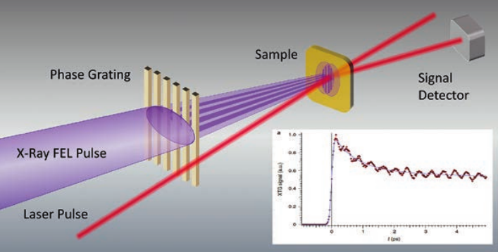
X-ray TG setup scheme: The XFEL pulse (in purple) is diffracted by a transmission phase grating, generating a Talbot carpet on the
sample, which induces a TG excitation with spatial periodicity. A delayed optical pulse (in red) monitors the temporal evolution of the
XTG via transient diffraction. In the inset, XTG signal from a bismuth germinate sample at 7.1 keV with an excitation grating pitch of
770 nm. The fast oscillations are attributed to a coherent optical phonon.

